Fused quartz wafers are critical in the semiconductor industry due to their high purity, thermal stability, and excellent electrical insulation properties.
Fused quartz wafers are critical in the semiconductor industry due to their high purity, thermal stability, and excellent electrical insulation properties. As an amorphous form of SiO2, they are ideal for high-temperature processes like chemical vapor deposition (CVD) and epitaxial growth. Their high transparency in ultraviolet (UV) and infrared (IR) spectra also makes them suitable for photolithography, etching masks, and optical components. Additionally, fused quartz wafers are increasingly used in laser applications, where their low absorption and high damage threshold are essential for precision laser machining and laser optics fabrication.
CQT Group is a leading manufacturer of fused quartz wafers, offering a wide range of capabilities to meet diverse industry needs. We produce wafers in sizes from 2 to 12 inches in diameter, and can also create square wafers upon request. Custom thicknesses are available, with the thinnest wafers being approximately 100 microns. Our manufacturing process is supported by state-of-the-art equipment, including surface inspection tools like optical profilers and wafer defect inspection systems. We operate in a Class 1000 cleanroom environment, ensuring the highest quality standards for our products.
| Parameter | JGS2 |
| Maximum Size | <Φ300mm |
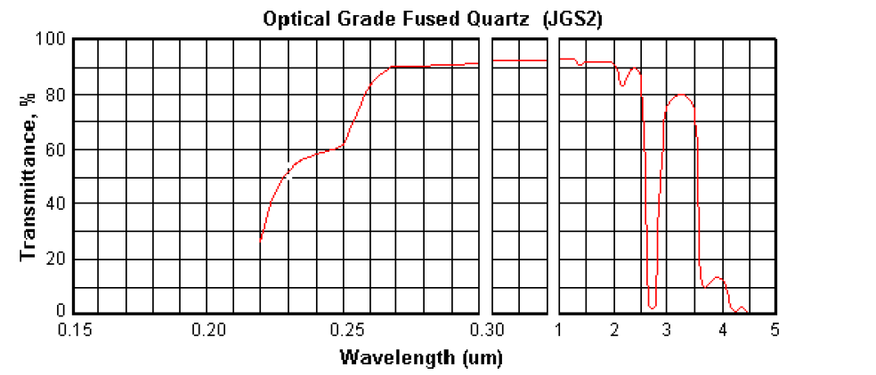
| Transmission Range | 0.26~2.10um |
| (Medium transmission ratio) | (Tavg>85%) |
| OH- Content | 150ppm |
| Fluorescence (ex 254nm) | Strong v-b |
| Impurity Content | 20-40 ppm |
| Birefringence Constant | 4-6nm/cm |
| Melting Method | Oxy-hydrogen melting |
| Applications | Semiconductor and high temperature window |

The general specs are as follows sheet, if your specified is not included with it, you may freely tell us and we’ll pleased to customize them for you.
| spec | unit | 4" | 6" | 8" | 10" | 12” |
| Diameter/size(or square) | mm | 100 | 150 | 200 | 250 | 300 |
| Tolerance (±) | mm | 0.2 | 0.2 | 0.2 | 0.2 | 0.2 |
| Thickness | mm | 0.10 or more | 0.30 or more | 0.40 or more | 0.50 or more | 0.50 or more |
| Primary reference flat | mm | 32.5 | 57.5 | Semi-notch | Semi-notch | Semi-notch |
| LTV (5mmx5mm) | µm | < 0.5 | < 0.5 | < 0.5 | < 0.5 | < 0.5 |
| TTV | µm | < 2 | < 3 | <3 | <5 | <5 |
| Bow | µm | ±20 | ±30 | ±40 | ±40 | ±40 |
| Warp | µm | ≤ 30 | ≤ 40 | ≤ 50 | ≤ 50 | ≤ 50 |
| PLTV(5mm*5mm)<0.4um | % | ≥95% | ≥95% | ≥95% | ≥95% | ≥95% |
| Edge Rounding | mm | Compliant with SEMI M1.2 Standard/refer to IEC62276 | ||||
| Surface Type | Single Side Polished /Double Sides Polished | |||||
| Polished side Ra | nm | ≤1 | ||||
| Back Side Criteria | µm | general 0.2-0.7 or customized | ||||
Copyright © Hangzhou Freqcontrol
Electronic Technology Ltd.
All Rights Reserved | Sitemap |
Powered by 