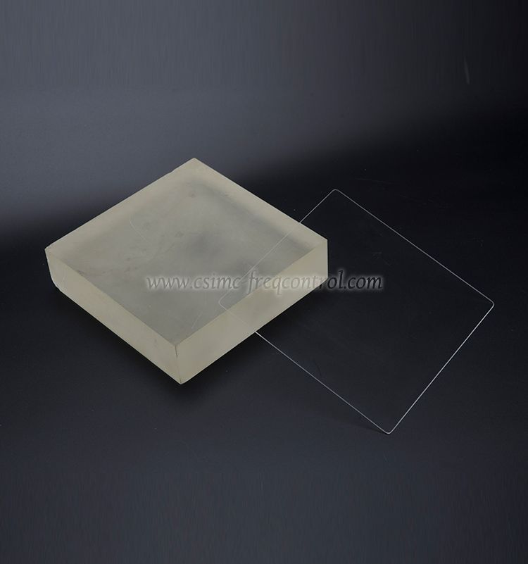
Let's take a look at the specifications of fused silica wafers!
JGS1 (Ultraviolet Grade Fused Silica)
These wafers show a high transparency in the ultraviolet spectral range. The transmission in the VIS and UV (down to approx. 215 nm) is approx. 90 percent (just reflection losses) and drops down to 0% in the spectral range between 215 and 150 nm. In the infrared range, the comparable high OH-concentration of typically 1000 ppm causes absorption bands for wavelengths > 1.2 μm.
JGS2 (Optical Grade Fused Silica)
As compared with JGS1 wafers, the transmission range of considerably more economical JGS2 wafers is shifted towards longer wavelengths: UV-absorption already starts under approx. 270 nm wavelength, whereas at the VIS and IR the transmission is approx. 90% up to approx. two μm wavelength due to the lower OH-concentration (typ < 300 ppm).
JGS3 (Total Spectrum Fused Silica)
These wafers which are costly when compared with JGS1, it reveal an extremely low OH-content (typ< 10 ppm) with a high transparency of > 80% over a wide spectral range of approx. 200 nm - 3 μm, and approx 90% at the wavelength range 250 - 2.5 μm.
Surfaces
Usually, fused silica wafers are double-side polished. The single-side polishing potential on request.
We are quartz materials manufacturer, welcome to contact us!

Copyright © Hangzhou Freqcontrol
Electronic Technology Ltd.
All Rights Reserved | Sitemap |
Powered by 