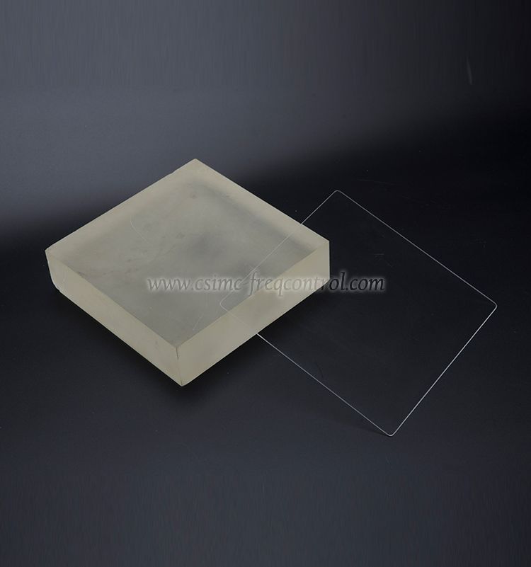
Silicon is widely found in rocks and gravel in the form of silicates or silica in nature. There are three major steps in the fabrication of fused silica wafers: silicon refining and purification, monocrystalline silicon growth, and wafer formation.
1. Silicon refining and purification
The purification of silicon is the first process. The sandstone raw material needs to be placed in an electric arc furnace with a carbon source of more than two thousand degrees Celsius. The reduction reaction is carried out at a high temperature to obtain metallurgical grade silicon, and then the pulverized metallurgical grade silicon is obtained. It reacts with gaseous hydrogen chloride to form a liquid silane and then passes through a distillation and chemical reduction process to obtain high-purity polycrystalline silicon.
2. Single crystal silicon growth
Wafer companies commonly use the Czochralski method. high-purity polysilicon is placed in a quartz crucible and heated continuously by a graphite heater surrounded by the outside. The temperature is maintained at about one thousand degrees Celsius. The air in the furnace is usually It is an inert gas that melts polysilicon without generating unwanted chemical reactions.
In order to form single crystal silicon, it is also necessary to control the direction of the crystal, the polysilicon melt is rotated, a seed crystal is immersed therein, and the seed crystal is rotated in the opposite direction by the pulling rod while slowly and vertically The ground is pulled up from the silicon melt.
The molten polycrystalline silicon adheres to the bottom end of the seed crystal and grows continuously in the direction in which the seed crystal lattice is arranged. After growth by the Czochralski method, the single crystal rod is cut to the appropriate size, then ground, and then chemically polished to at least one side as smooth as a mirror, at which point the wafer is completed.
The wafer manufacturer melts the polysilicon, implants the seed crystal in the melt, and then slowly pulls it out to form a cylindrical single crystal silicon ingot, which is determined by the orientation of the crystal ingot. The seed crystals are gradually formed in the molten silicon raw material.
3. Wafer molding
After completing the above two processes, the silicon ingot is further cut, barreled, sliced, chamfered, polished, laser engraved, and packaged, which becomes the basic material of the integrated circuit factory - silicon wafer, which is "crystal circle".
We are fused quartz wafers manufacturer, we can provide you with the most suitable products according to your needs, welcome to consult. In addition, we also have Tellurium Oxide for sale.

Copyright © Hangzhou Freqcontrol
Electronic Technology Ltd.
All Rights Reserved | Sitemap |
Powered by 