CQT uses a variety of glass and quartz depending on the application and material requirements. Our designers and engineers are skilled at working with any number of glass and quartz materials to machine and fabricate precision optical products such as fused quartz parts for optics, fused silica parts used in fiber optic applications
Fused silica wafers are highly valued in various optical applications due to their exceptional properties. These wafers come in different grades, each tailored for specific uses, such as deep ultraviolet (DUV) and infrared (IR) applications.
DUV Grade Fused Silica Wafers
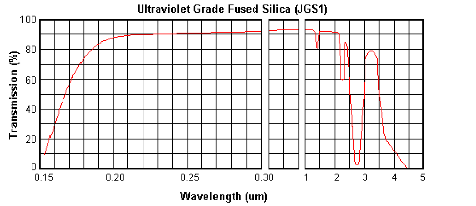
The UV grade fused silica wafers are made from fully synthetic materials with very low trace metal content, produced using the Synthetic Chemical Vapor Deposition (CVD) method. This process ensures the wafers have high purity and excellent optical properties. Fused silica is highly resistant to heat and exhibits a broad transmission range, with more than 85% transmission at 185 nm and over 90% from 200 nm to 2000 nm. Common brands and grades for UV grade fused silica include JGS1, Corning 7980, and SK1300. CQT Group supplies these wafers with diameters up to 8 inches (200 mm) and a surface roughness (Ra) of less than 0.5 nm, making them ideal for precision optical applications where minimal surface defects are crucial.
IR Grade Fused Silica Wafers
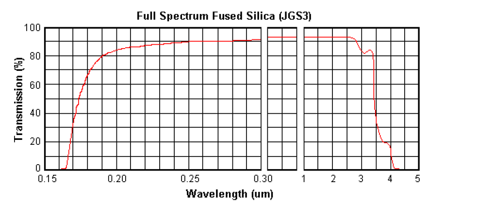
IR grade fused silica wafers are designed for applications requiring high transmission in the infrared range, typically from 185 nm to 3500 nm. These wafers have very low hydroxyl (OH) content, usually less than 5 ppm, which minimizes absorption in the IR region. The electrical melting method is used to produce IR grade fused silica, ensuring a high level of purity and consistency. Common brands and grades for IR grade fused silica include JGS3, Corning 7979, and SK1310. CQT Group supplies these wafers with diameters up to 8 inches (200 mm) and a surface roughness (Ra) of less than 0.5 nm, making them suitable for high-precision IR optical components and applications where low OH content is essential for performance.
| Parameter | JGS1 | JGS3 |
| Maximum Size | <Φ250mm | <Φ200mm |
| Transmission Range | 0.17~2.10um | 0.25~3.50um |
| (Medium transmission ratio) | (Tavg>90%) | (Tavg>85%) |
| OH- Content | 1200 ppm | 5ppm |
| Fluorescence (ex 254nm) | Virtually Free | Strong v-b |
| Impurity Content | 5 ppm | 40-50 ppm |
| Birefringence Constant | 2-4 nm/cm | 4-10nm/cm |
| Melting Method | Synthetic CVD | Electrical melting |
| Applications | Laser substrate:Window,lens,prism, mirror, etc. | IR substrate |


The general specs are as follows sheet, if your specified is not included with it, you may freely tell us and we’ll pleased to customize them for you.
| spec | unit | 4" | 6" | 8" | 10" | 12” |
| Diameter/size(or square) | mm | 100 | 150 | 200 | 250 | 300 |
| Tolerance (±) | mm | 0.2 | 0.2 | 0.2 | 0.2 | 0.2 |
| Thickness | mm | 0.10 or more | 0.30 or more | 0.40 or more | 0.50 or more | 0.50 or more |
| Primary reference flat | mm | 32.5 | 57.5 | Semi-notch | Semi-notch | Semi-notch |
| LTV (5mmx5mm) | µm | < 0.5 | < 0.5 | < 0.5 | < 0.5 | < 0.5 |
| TTV | µm | < 2 | < 3 | <3 | <5 | <5 |
| Bow | µm | ±20 | ±30 | ±40 | ±40 | ±40 |
| Warp | µm | ≤ 30 | ≤ 40 | ≤ 50 | ≤ 50 | ≤ 50 |
| PLTV(5mm*5mm)<0.4um | % | ≥95% | ≥95% | ≥95% | ≥95% | ≥95% |
| Edge Rounding | mm | Compliant with SEMI M1.2 Standard/refer to IEC62276 | ||||
| Surface Type | Single Side Polished /Double Sides Polished | |||||
| Polished side Ra | nm | ≤1 | ||||
| Back Side Criteria | µm | general 0.2-0.7 or customized | ||||
Copyright © Hangzhou Freqcontrol
Electronic Technology Ltd.
All Rights Reserved | Sitemap |
Powered by 